GLT6400M16 View Datasheet(PDF) - G-Link Technology
Part Name
Description
View to exact match
GLT6400M16 Datasheet PDF : 13 Pages
| |||
G-LINK
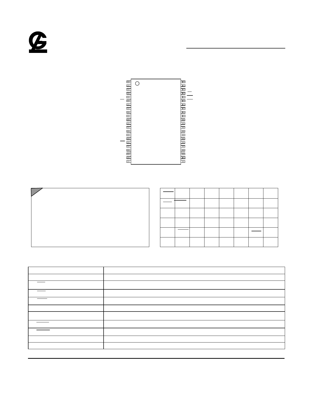
Pin Configurations :
GLT6400M16
Ultra Low Power 256k x 16 CMOS SRAM
May 2001(Rev. 2.0)
GLT6400M16
48 Ball fpBGA :
A4
1
A3
2
A2
3
A1
4
A0
5
CE1
6
I/O0
7
I/O1
8
I/O2
9
I/O3
10
Vcc 11
Vss 12
I/O4
13
I/O5
14
I/O6
15
I/O7
16
WE 17
A17
18
A16
19
A15
20
A14
21
A13
22
44
A5
43
A6
42
A7
41
OE
40
BHE
39
BLE
38
I/O15
37
I/O14
36
I/O13
35
I/O12
34
Vss
33
Vcc
32
I/O11
31
I/O10
30
I/O9
29
I/O8
28
NC
27
A8
26
A9
25
A10
24
A11
23
A12
A
BCDE F
¡¡ ¡ ¡ ¡ ¡
¡¡ ¡ ¡ ¡ ¡
¡ ¡ ¡¡ ¡¡
¡ ¡ ¡¡ ¡¡
¡ ¡ ¡¡ ¡¡
¡ ¡ ¡¡ ¡¡
(Bottom View)
Pin Descriptions:
Name
A0 – A17
CE 1 and CE2
OE
WE
I/O0 – I/O15
VCC
BLE
BHE
GND
NC
GH
ABCDE FGH
¡
¡
1
BLE I/O9 I/O10 Vss
Vcc I/O15 I/O16 NC
¡¡
2
OE BHE I/O11 I/O12 I/O13 I/O14 NC
A8
¡ ¡ 3 A0
A3
A5 A17 NC A14 A12 A9
¡ ¡ 4 A1
A4
A6
A7 A16 A15 A13 A10
¡¡5
A2
CE1 I/O2 I/O4 I/O5 I/O6 WE A11
¡ ¡ 6 CE2 I/O1 I/O3 Vcc Vss I/O7 I/O8 NC
(Bottom View)
Note : NC means no Ball.
Function
Address Inputs
Chip Enable Input
Output Enable Input
Write Enable Input
Data Input and Data Output
2.5V Power Supply
Lower Byte Enable Input ( I/O0 to I/O7)
Higher Byte Enable Input ( I/O8 to I/O15)
Ground
No Connection
G-Link Technology Corporation
2701 Northwestern Parkway
Santa Clara, CA 95051, U.S.A.
-2-
G-Link Technology Corporation, Taiwan
6F No. 24-2, Industry E. RD. IV, Science Based
Industrial Park, Hsin Chu, Taiwan.
Share Link: 