UPC8139GR-7JH View Datasheet(PDF) - NEC => Renesas Technology
Part Name
Description
View to exact match
UPC8139GR-7JH Datasheet PDF : 20 Pages
| |||
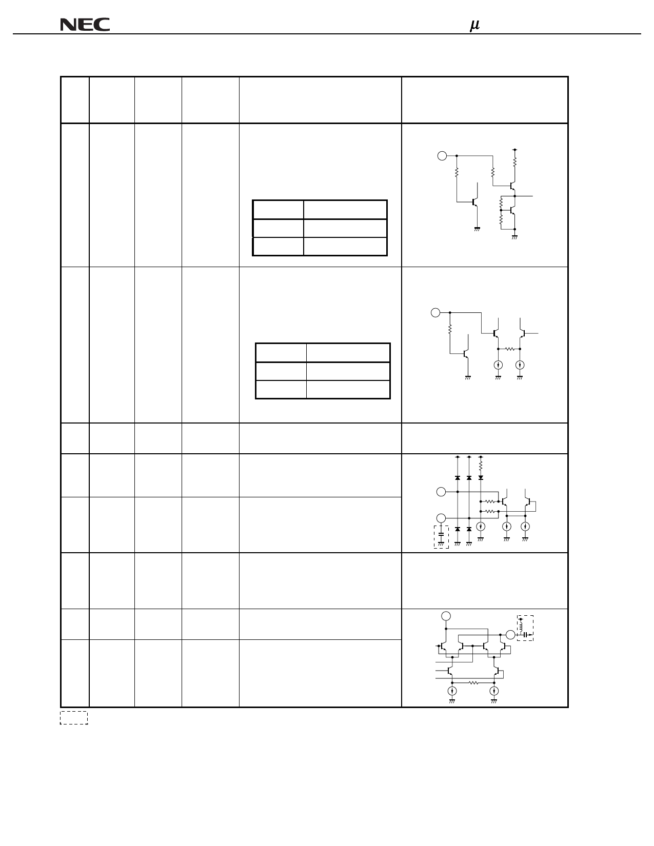
PIN FUNCTIONS
Pin Symbol
No.
Applied
Voltage
(V)
23
VPS (RX)
0 to VCC
Pin
Note
Voltage
(V)
–
Function and Description
Power save pin for the receiver block
(IF amplifier, RSSI, 2nd down
converter). This pin is interlocked to
the internal regulator and can control
the following.
VPS (V)
IC stat
2.5 to VCC ON (Active Mode)
0 to 0.3 OFF (Sleep Mode)
24
VPS (TX)/
0 to VCC
–
Power save pin for the transmitter
VAGC
block (quadrature modulator, up
converter, AGC circuit). This pin is
interlocked to the internal regulator
and can control the following.
VPS (V)
IC stat
0.9 to VCC ON (Active Mode)
0 to 0.5 OFF (Sleep Mode)
25
VCC5
26 TX MIX-
LOinb
2.7 to
4.0
–
28 TX MIX-
–
LOin
–
Supply voltage for the AGC block.
2.0
Bypass pin for the local input of the up
converter. Ground this pin through an
external capacitor.
2.0
Local input pin for the up converter.
High impedance input.
27 GND5
0
29
VCC6
30
TX
MIXout
2.7 to
4.0
2.7 to
4.0
–
Ground pin for the AGC and up
converter. Form as wide a ground
pattern as possible to minimize its
impedance.
–
Supply voltage pin for the up converter
block.
–
RF output pin for the up converter
block. This is an open collector
output, so an impedance matching
circuit should be attached externally.
: External attachment
Note The pin voltage is measured on Vcc=3.0 V.
µPC8139GR-7JH
Internal Equivalent Circuit
23
24
28
26
29
30
10
Preliminary Data Sheet
Share Link: 