SCY99080CDWR2G View Datasheet(PDF) - ON Semiconductor
Part Name
Description
View to exact match
SCY99080CDWR2G
ON Semiconductor

SCY99080CDWR2G Datasheet PDF : 27 Pages
| |||
DDA002C
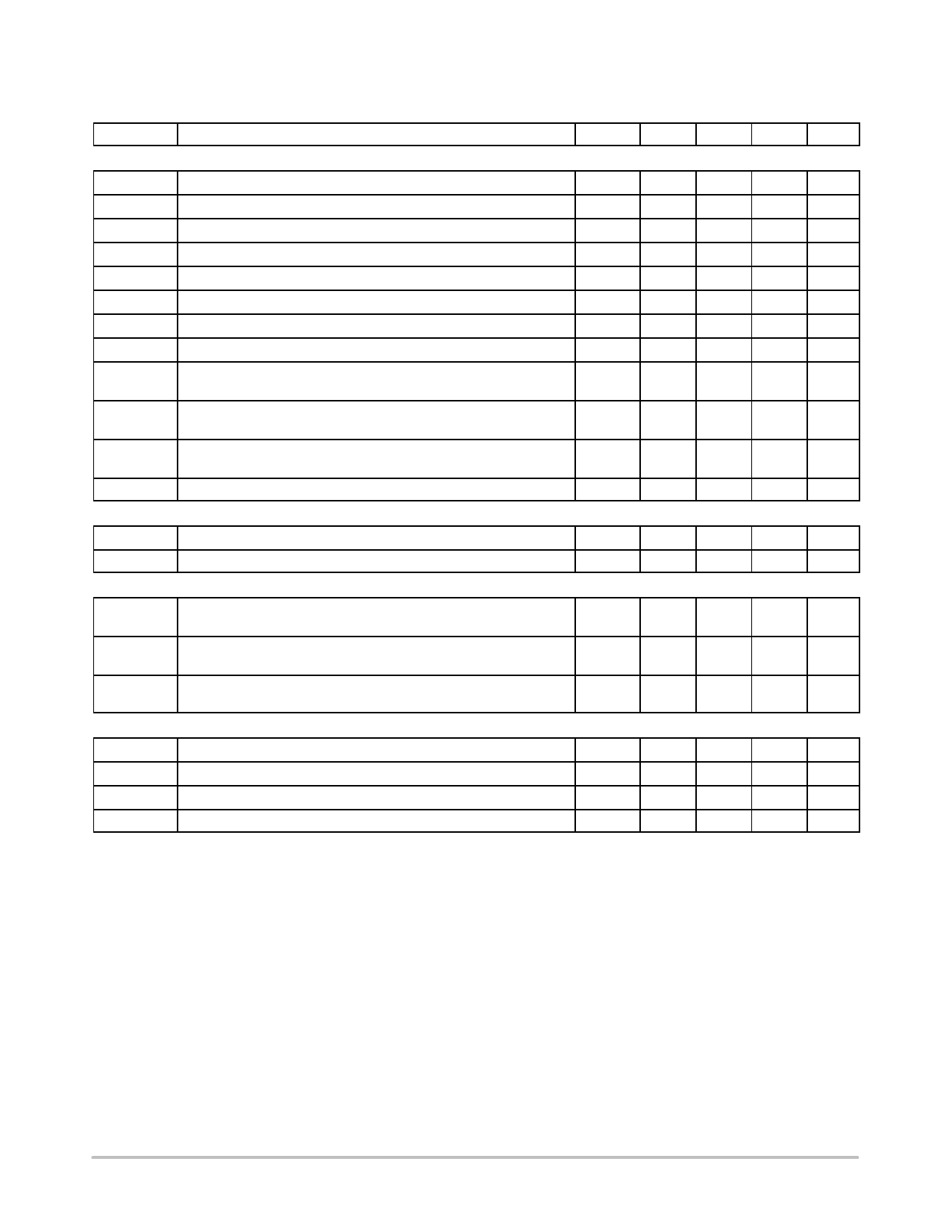
Electrical Characteristics
(For typical values Tj = 25°C, for min/max values Tj = −40°C to +125°C, Vcc = 15 V unless otherwise noted)
Symbol
Rating
Pin
Min
Typ
Max Unit
LOW IMPEDANCE DRIVE OUTPUTS (HGD, LGD)
Tr – Hgd
Output voltage rise−time @ CL = 1 nF, 10−90% of output signal
18, 17
−
80
−
ns
Tf – Hgd
Output voltage fall−time @ CL = 1 nF, 10−90% of output signal
18, 17
−
40
−
ns
ROH – Hgd
Source resistance – (Note 9)
18, 17
−
30
−
Ω
ROL − Hgd
Sink resistance – (Note 9)
18, 17
−
15
25
Ω
Tr – Lgd
Output voltage rise−time @ CL 1 nF, 10−90% of output signal
15, 14
−
80
−
ns
Tf – Lgd
Output voltage fall−time @ CL = 1 nF, 10−90% of output signal
15, 14
−
40
−
ns
ROH – Lgd
Source resistance (Note 9)
15, 14
−
30
−
Ω
ROL − Lgd
Sink resistance (Note 9)
15, 14
−
15
25
Ω
T_dead−min
Minimum dead−time, RDT = 2.7 kΩ from pin 9 to GND
(Notes 20 and 21)
9
−
100
−
ns
T_dead−nom
Nominal dead−time with RDT = 10 kΩ from pin 9 to GND
(Notes 20 and 21)
9
245
300
355
ns
T_dead−max
Maximum dead−time with RDT = 82 kΩ from pin 9 to GND
(Notes 20 and 21)
9
−
2
−
ms
IHV_LEAK
Leakage current on high voltage pins to GND (Note 10)
17, 18, 19 −
−
5
mA
SYNCHRONIZATION DRIVE OUTPUTS (LGS AND HGS)
ROH – S
Source resistance
ROL – S
Sink resistance
DGS (SYNCHRONOUS OUTPUT CLAMP)
12, 13, 14 −
60
−
Ω
12, 13, 14 −
60
−
Ω
Tdgs
Clamped on−time duration, Rdgs = 48 kΩ, Fsw < 24 kHz,
DT = 300 ns (Notes 11, 20 and 21)
3, 12, 13 17.1 17.9 18.7
ms
Iduty_min
Minimum on−time duration, Rdgs = 12 kΩ, Fsw = Fmin
(Notes 11, 20 and 21)
3, 12, 13 4.45 4.66 4.87
ms
Iduty_nom
Minimum on−time duration, Rdgs = 26 kΩ, Fsw < 24 kHz
(Notes 11, 20 and 21)
3, 12, 13 9.65
10
10.35
ms
TIMERS
CIG_I
CIG timer charging current
2
−
10
−
mA
CIG_E
CIG timer ending voltage (Note 12)
2
−
5
−
V
CIG_t
Typical CIG duration for a 0.22 mF capacitor on CIG pin
2
−
110
−
ms
SS_E
Soft−start ending voltage (Note 13)
4
−
1.9
−
V
4. VCC(min) = VCCreset
5. Outputs Lgs and Hgs (pin 9/10) are unloaded.
6. Guaranteed by design.
7. DCsh = (DChs/(DChs + DCls)) * 100%, DCsl = (DCls/(DChs + DCls)) * 100%
8. The VFB_DC_0 is the FB voltage below which are all outputs disabled.
The FB voltage has to increases to VFB_DC_0 + VFB_DC_0_Hyste to re−enable all outputs of the controller.
9. Low impedance source and sink RDS(on) are designed to respectively deliver 0.5 A and −1 A at Tj = 100°C.
10. Pins 17, 18 and 19 are on the same potencial during IHV_LEAK measurements
11. On−time on synchro outputs wont be longer than on−time on power outputs.
12. The soft start pin is pulled down by an internal switch until the CIG timer ending voltage is reached
13. FB timer is disabled until the soft−start ending voltage is reached
14. EN1 input is blanked until the preheat period (CIG) ends. The OTP input is blanked during full startup sequence made of: PFC_del + CIG_t + SS_t
15. The FB timeout circuit starts to operate at the end of PFC_del + CIG_t + SS_t period.
16. An NTC resistor of 8.8 kW @ TA = 110°C is connected to ground.
17. The EN1 and EN2 input voltages have to go 50 mV below VEN1, VEN2 to release these inputs.
18. The OTP input voltage has to go 50 mV above OTPref_V to release this input.
19. The R_Fmin pin do not accept any bypass capacitor
20. Maximum acceptable capacitance connected to the pin is 100 pF
21. Measured for VCC = 10.5 V
http://onsemi.com
7
Share Link: