TC7MPN3125FTGEB View Datasheet(PDF) - Toshiba
Part Name
Description
View to exact match
TC7MPN3125FTGEB Datasheet PDF : 22 Pages
| |||
TC7MPN3125FTG
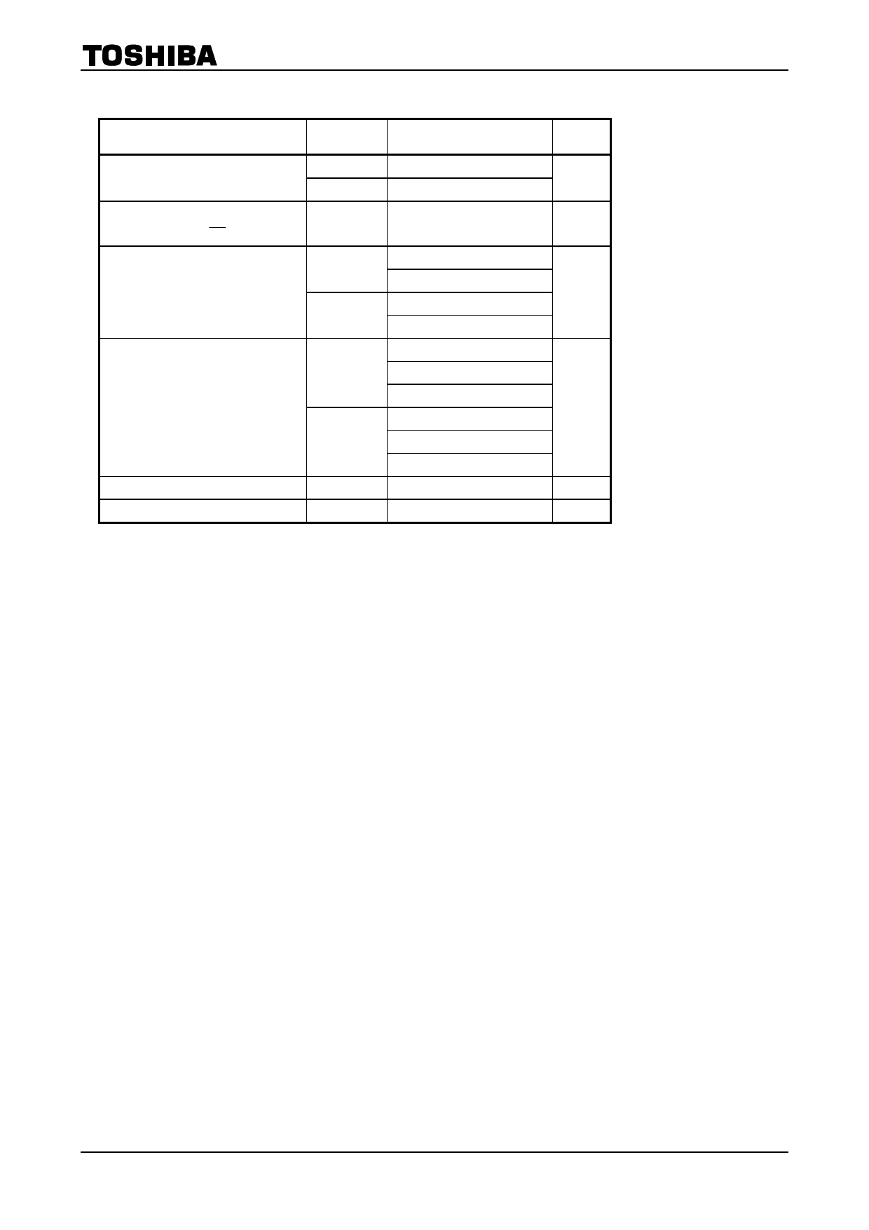
Operating Ranges (Note 1)
Characteristics
Symbol
Rating
Unit
Power supply voltage
Input voltage
(DIR, OE )
Bus I/O voltage
(Note 2)
VCCA
VCCB
VIN
VI/OA
VI/OB
Output current
Operating temperature
Input rise and fall time
IOUTA
IOUTB
Topr
dt/dv
1.1 to 2.7
V
1.65 to 3.6
0 to 3.6
V
0 to 3.6 (Note 3)
0 to VCCA (Note 4)
0 to 3.6 (Note 3)
0 to VCCB (Note 4)
±9
(Note 5)
±3
(Note 6)
±1
(Note 7)
±3
(Note 8)
±2
(Note 9)
±0.5 (Note 10)
−40 to 85
0 to 10 (Note 11)
V
mA
°C
ns/V
Note 1:
The operating ranges must be maintained to ensure the normal operation of the device. Unused inputs and
bus inputs must be tied to either VCC or GND. Please connect both bus inputs and the bus outputs with
VCC or GND when the I/O of the bus terminal changes by the function. In this case, please note that the
output is not short-circuited.
Note 2: Don’t use in VCCA > VCCB
Note 3: Output in OFF state
Note 4: High or low state
Note 5: VCCB= 2.3 to 2.7 V
Note 6: VCCB = 1.65 to 1.95 V
Note 7: VCCB = 1.4 to 1.6 V
Note 8: VCCA = 3.0 to 3.6 V
Note 9: VCCA = 2.3 to 2.7 V
Note 10: VCCA = 1.65 to 1.95 V
Note 11: VIN = 0.8 to 2.0 V, VCCA = 2.5 V, VCCB = 3.0 V
5
2007-10-19
Share Link: 