NTE1934 View Datasheet(PDF) - NTE Electronics
Part Name
Description
View to exact match
NTE1934 Datasheet PDF : 2 Pages
| |||
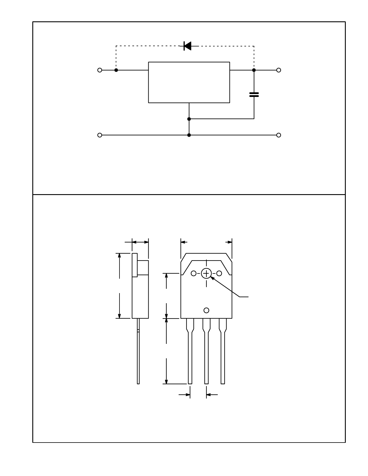
VIN
DC Input
External Circuit
D1
2
1
+
3
– C1 VO
DC Output
Note 1. Output capacitor C1 (47 to 100µf) shall be connected directly to output terminal (Pin1)
and GND terminal (PIn3) as shown above.
Note 2. When wiring between the regulator and the load is long, another capacitor (47 to 100µf)
shall be added in parallel with the load.
Note 3. If there is a possibility of reverse biasing between input and output, a protection diode
(D1) is to be added. The recommended diode for D1 is NTE116.
.190 (4.82)
.787
(20.0)
.615 (15.62)
VIN
.591
(15.02)
.126 (3.22)
Dia
.787
(20.0)
VO VIN
GND
.215 (5.47)
Share Link: 