PCK2010RDL View Datasheet(PDF) - Philips Electronics
Part Name
Description
View to exact match
PCK2010RDL Datasheet PDF : 18 Pages
| |||
Philips Semiconductors
CK98R (100/133MHz) RCC spread spectrum
system clock generator
Product specification
PCK2010R
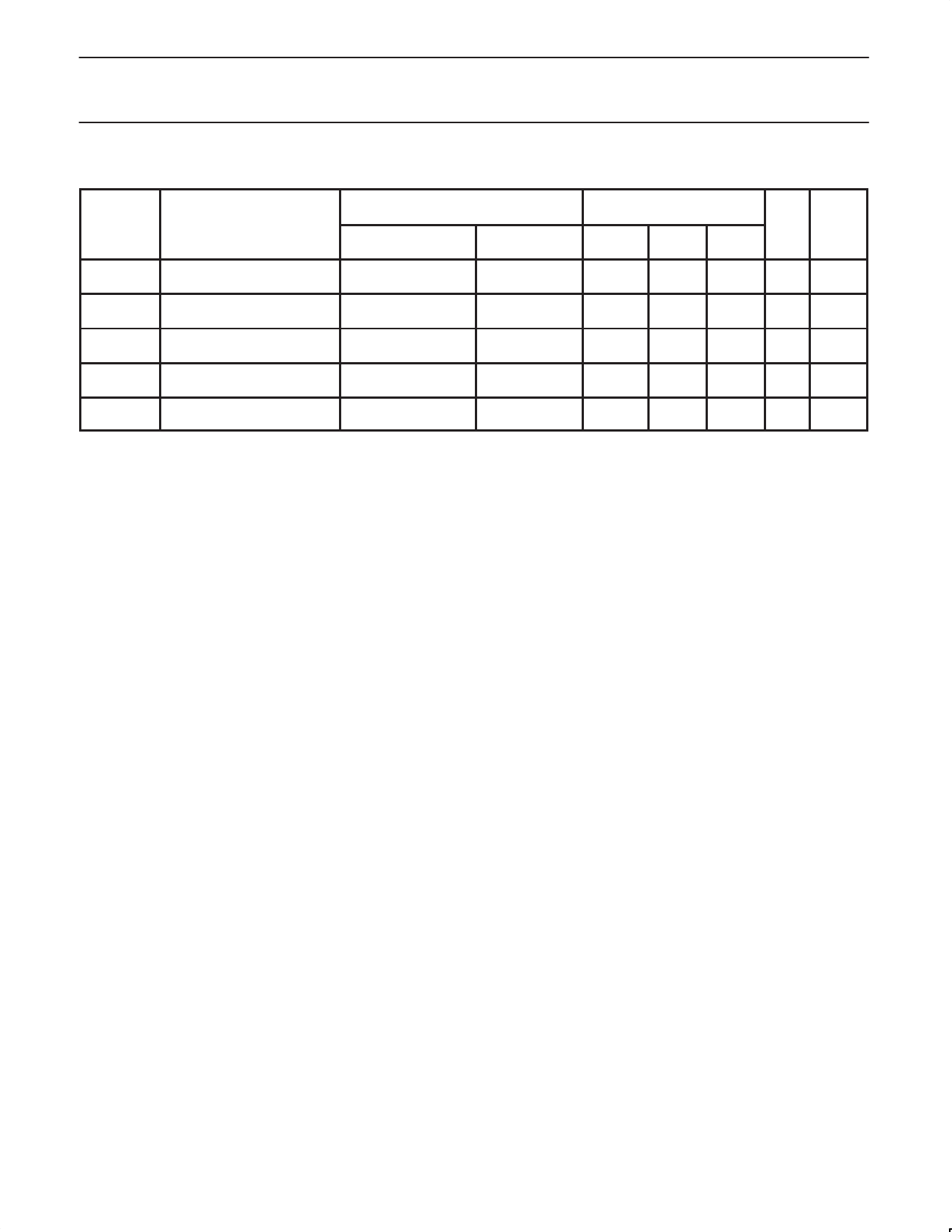
AC CHARACTERISTICS (Continued)
SYMBOL
THPOFFSET
THPOFFSET
THPOFFSET
THPOFFSET
THPOFFSET
PARAMETER
CPUCLK to 3V66 CLK,
CPU leads
3V66 CLK to PCICLK,
3V66 leads
CPUCLK to IOAPIC,
CPU leads
CPUCLK to PCICLK ,
CPU leads
CPUDIV2 to CPUCLK,
CPUDIV2 leads
TEST CONDITIONS
Measurement loads
(lumped)
CPU@20 pF,
3V66@30 pF
3V66@30 pF,
PCI@30 pF
CPU@20 pF,
IOAPIC@20 pF
CPU@20 pF
PCI@30 pF
CPUDIV2@20 pF
CPU@20 pF
Measure points
CPU@1.25 V,
3V66@1.5 V
3V66@1.5 V,
PCI@1.5 V
3CPU@1.25 V,
IOAPIC@1.25 V
CPU@1.25 V
PCI@1.5 V
CPUDIV2@
CPU@1.25 V
LIMITS
Tamb = 0°C to +70°C
MIN
TYP
MAX
UNIT NOTES
0.0
0.45
1.5
ns
1
1.5
2.0
3.5
ns
1
1.5
2.4
4.0
ns
1
1.5
3.8
4.0
ns
0.0
1.6
2.5
ns
NOTES:
1. Output drivers must have monotonic rise/fall times through the specified VOL/VOH levels.
2. Period, jitter, offset and skew measured on rising edge @1.25 V for 2.5 V clocks and @ 1.5 V for 3.3 V clocks.
3. The PCICLK is the CPUCLK divided by four at CPUCLK = 133 MHz. The 3V66 CLK is internal VCO frequency divided by three at
CPUCLK = 100 MHz.
4. 3V66 CLK is internal VCO frequency divided by two at CPUCLK = 133 MHz. The 3V66 CLK is internal VCO frequency divided by three at
CPUCLK = 100 MHz.
5. THKH is measured at 2.0 V for 2.5 V outputs, 2.4 V for 3.3 V outputs as shown in Figure 4.
6. THKL is measured at 0.4 V for all outputs as shown in Figure 4.
7. The time is specified from when VDDQ achieves its nominal operating level (typical condition VDDQ = 3.3 V) until the frequency output is
stable and operating within specification.
8. THRISE and THFALL are measured as a transition through the threshold region VOL = 0.4 V and VOH = 2.4 V (1 mA) JEDEC specification.
9. The average period over any 1 µs period of time must be greater than the minimum specified period.
10. Calculated at minimum edge-rate (1V/ns) to guarantee 45/55% duty-cycle. Pulse width is required to be wider at faster edge-rate to ensure
duty-cycle specification is met.
11. Output (see Figure 5 for measure points).
1999 Oct 19
10
Share Link: 