IDT723612L30PQF View Datasheet(PDF) - Integrated Device Technology
Part Name
Description
View to exact match
IDT723612L30PQF Datasheet PDF : 25 Pages
| |||
IDT723612
CMOS SYNCBiFIFOTM 64 x 36 x 2
COMMERCIAL AND INDUSTRIAL
TEMPERATURE RANGES
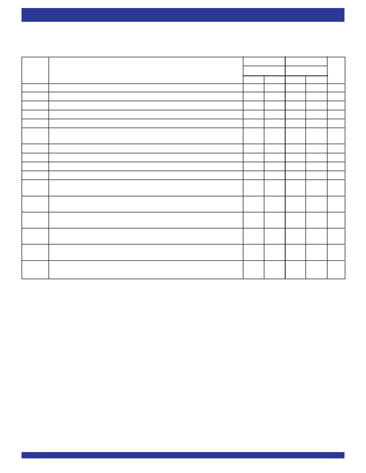
SWITCHING CHARACTERISTICS OVER RECOMMENDED RANGES OF SUPPLY
VOLTAGE AND OPERATING FREE-AIR TEMPERATURE, CL = 30PF
(Commercial: VCC = 5.0V ±10%, TA = 0°C to +70°C; Industrial; VCC = 5.0V ± 10%,TA = 40°C to +85°C)
Symbol
tA
tWFF
tREF
tPAE
tPAF
tPMF
tPMR
tMDV
tPDPE
tPOPE
tPOPB(4)
tPEPE
tPEPB(4)
tRSF
tEN
tDIS
Parameter
Access Time, CLKA↑ to A0-A35 and CLKB↑ to B0-B35
Propagation Delay Time, CLKA↑ to FFA and CLKB↑ to FFB
Propagation Delay Time, CLKA↑ to EFA and and CLKB↑ to EFB
Propagation Delay Time, CLKA↑ to AEA and CLKB↑ to AEB
Propagation Delay Time, CLKA↑ to AFA and CLKB↑ to AFB
Propagation Delay Time, CLKA↑ to MBF1 LOW or MBF2 HIGH and CLKB↑ to
MBF2 LOW or MBF1 HIGH
Propagation Delay Time, CLKA↑ to B0-B35(2) and CLKB↑ to A0-A35(3)
Propagation Delay Time, MBA to A0-A35 valid and MBB to B0-B35 valid
Propagation Delay Time, A0-A35 valid to PEFA valid; B0-B35 valid to PEFB valid
Propagation Delay Time, ODD/EVEN to PEFA and PEFB
Propagation Delay Time, ODD/EVEN to parity bits (A8, A17, A26, A35) and
(B8, B17, B26, B35)
Propagation Delay Time, W/RA, CSA, ENA, MBA or PGA to PEFA; W/RB, CSB,
ENB, MBB, PGB to PEFB
Propagation Delay Time, W/RA, CSA, ENA, MBA or PGA to parity bits ( A8, A17, A26, A35);
W/RB, CSB, bits (B8, B17, B26, B35) ENB, MBB or PGB to parity
Propagation Delay Time, RST to (AEA, AEB) LOW and (AFA, AFB, MBF1, MBF2)
HIGH
Enable Time, CSA and W/RA LOW to A0-A35 active and CSB LOW and W/RB HIGH
to B0-B35 active
Disable Time, CSA or W/RA HIGH to A0-A35 at high impedance and CSB HIGH
or W/RB LOW to B0-B35 at high impedance.
Commercial Com’l & Ind’l(1)
IDT723612L15 IDT723612L20
Min. Max. Min. Max. Unit
2
10
2
12 ns
2
10
2
12 ns
2
10
2
12 ns
2
10
2
12 ns
2
10
2
12 ns
1
9
1
12 ns
3
11
1
11
3
10
3
11
2
11
3
13 ns
1
11.5 ns
3
11 ns
3
12 ns
2
12 ns
1
11
1
12 ns
3
12
3
13 ns
1
15
1
20 ns
2
10
2
12 ns
1
8
1
9 ns
NOTES:
1. Industrial temperature range product for 20ns speed grade is available as a standard device. All other speed grades are available by special order.
2. Writing data to the mail1 register when the B0-B35 outputs are active and MBB is HIGH.
3 Writing data to the mail2 register when the A0-A35 outputs are active and MBA is HIGH.
4. Only applies when reading data from a mail register.
9
FEBRUARY 13, 2009
Share Link: 