UT61L6416MC-12 View Datasheet(PDF) - Utron Technology Inc
Part Name
Description
View to exact match
UT61L6416MC-12 Datasheet PDF : 9 Pages
| |||
Rev. 1.0
UTRON
UT61L6416
64K X 16 BIT HIGH SPEED CMOS SRAM
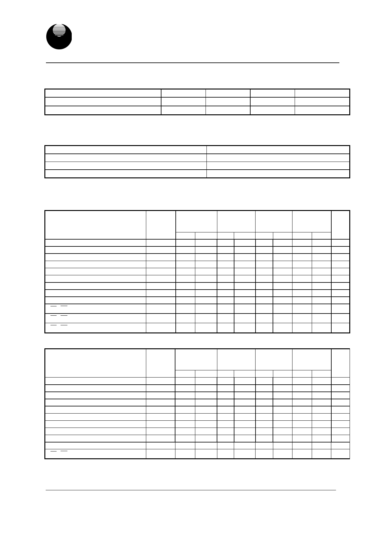
CAPACITANCE (TA=25℃, f=1.0MHz)
PARAMETER
SYMBOL
MIN.
MAX
Input Capacitance
CIN
-
6
Input/Output Capacitance
CI/O
-
8
Note : These parameters are guaranteed by device characterization, but not production tested.
AC TEST CONDITIONS
UNIT
pF
pF
Input Pulse Levels
Input Rise and Fall Times
Input and Output Timing Reference Levels
Output Load
0V to 3.0V
3ns
1.5V
CL = 30pF, IOH/IOL = -4mA / 8mA
AC ELECTRICAL CHARACTERISTICS (TA =0℃ to 70℃)
(1) READ CYCLE
PARAMETER
Read Cycle Time
Address Access Time
Chip Enable Access Time
Output Enable Access Time
Chip Enable to Output in Low Z
Output Enable to Output in Low Z
Chip Disable to Output in High Z
Output Disable to Output in High Z
Output Hold from Address Change
LB , UB Access Time
LB , UB to High Z Output
LB , UB to Low Z Output
UT61L6416 UT61L6416 UT61L6416 UT61L6416
SYMBOL
-8
-10
VCC=3.15〜3.6 VCC=3.0〜3.6
-12
-15
VCC=3.0〜3.6 VCC=3.0〜3.6
UNIT
MIN. MAX. MIN. MAX. MIN. MAX. MIN. MAX.
tRC
tAA
tACE
tOE
tCLZ*
tOLZ*
tCHZ*
tOHZ*
tOH
8
-
10
-
12 -
15
-
ns
-
8
-
10
- 12
-
15 ns
-
8
-
10
- 12
-
15 ns
-
4
-
5
-
6
-
7 ns
3
-
3
-
3
-
3
-
ns
0
-
0
-
0
-
0
-
ns
-
4
-
5
-
6
-
7 ns
-
4
-
5
-
6
-
7 ns
3
-
3
-
3
-
3
-
ns
tBA
-
4
-
5
-
6
-
7 ns
tBHZ
-
4
-
5
-
6
-
7 ns
tBLZ
0
-
0
-
0
-
0
-
ns
(2) WRITE CYCLE
UT61L6416 UT61L6416 UT61L6416 UT61L6416
PARAMETER
SYMBOL
-8
VCC=3.15〜3.6
-10
-12
-15
VCC=3.0〜3.6 VCC=3.0〜3.6 VCC=3.0〜3.6
MIN. MAX. MIN. MAX. MIN. MAX. MIN. MAX.
Write Cycle Time
Address Valid to End of Write
Chip Enable to End of Write
Address Set-up Time
Write Pulse Width
Write Recovery Time
Data to Write Time Overlap
Data Hold from End of Write Time
Output Active from End of Write
Write to Output in High Z
tWC
8
-
10
-
12 -
15
-
tAW
7
-
8
-
9
-
10
-
tCW
7
-
8
-
9
-
10
-
tAS
0
-
0
-
0
-
0
-
tWP
7
-
8
-
9
-
10
-
tWR
0
-
0
-
0
-
0
-
tDW
5.5
-
6
-
7
-
8
-
tDH
0
-
0
-
0
-
0
-
tOW*
3
-
3
-
3
-
3
-
tWHZ*
-
4
-
5
-
6
-
7
LB , UB Valid to End of Write
tBW
7
-
8
-
9
-
10
-
*These parameters are guaranteed by device characterization, but not production tested.
UNIT
ns
ns
ns
ns
ns
ns
ns
ns
ns
ns
ns
UTRON TECHNOLOGY INC.
1F, No. 11, R&D Rd. II, Science-Based Industrial Park, Hsinchu, Taiwan, R. O. C.
TEL: 886-3-5777882 FAX: 886-3-5777919
4
P80072
Share Link: 