MM74HCT373 View Datasheet(PDF) - Fairchild Semiconductor
Part Name
Description
View to exact match
MM74HCT373 Datasheet PDF : 10 Pages
| |||
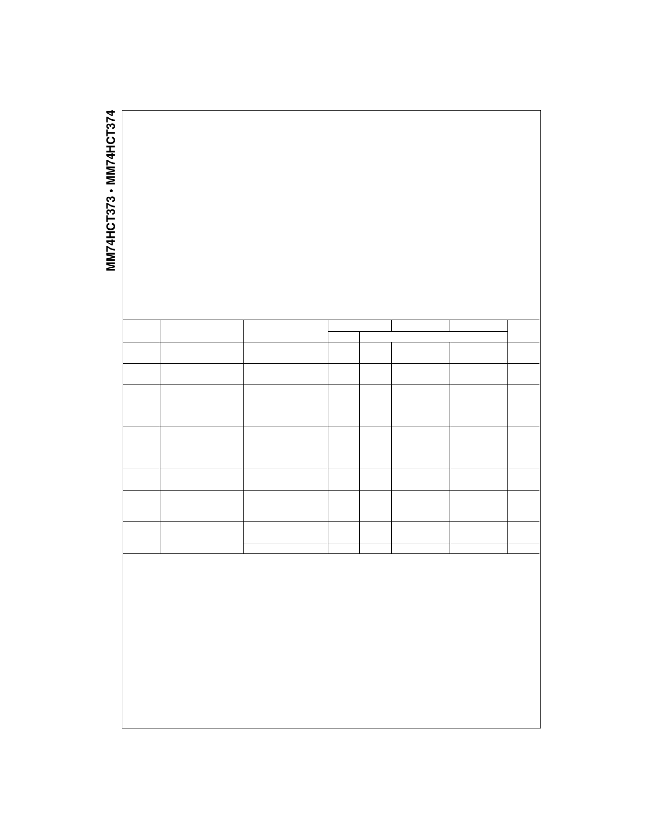
Absolute Maximum Ratings(Note 1)
(Note 2)
Supply Voltage (VCC)
DC Input Voltage (VIN)
DC Output Voltage (VOUT)
Clamp Diode Current (IIK, IOK)
DC Output Current, per pin (IOUT)
DC VCC or GND Current, per pin (ICC)
Storage Temperature Range (TSTG)
Power Dissipation (PD)
(Note 3)
S.O. Package only
Lead Temperature (TL)
(Soldering 10 seconds)
0.5 to 7.0V
1.5 to VCC 1.5V
0.5 to VCC 0.5V
r20 mA
r35 mA
r70 mA
65qC to 150qC
600 mW
500 mW
260qC
Recommended Operating
Conditions
Min Max Units
Supply Voltage (VCC)
4.5 5.5
V
DC Input or Output Voltage
0
VCC
V
(VIN, VOUT)
Operating Temperature Range (TA) 40 85 qC
Input Rise or Fall Times
(tr, tf)
500 ns
Note 1: Absolute Maximum Ratings are those values beyond which dam-
age to the device may occur.
Note 2: Unless otherwise specified all voltages are referenced to ground.
Note 3: Power Dissipation temperature derating — plastic “N” package:
12 mW/qC from 65qC to 85qC.
DC Electrical Characteristics
VCC 5V r 10% (unless otherwise specified)
Symbol
Parameter
Conditions
VIH
Minimum HIGH Level
Input Voltage
VIL
Maximum LOW Level
Input Voltage
VOH
Minimum HIGH Level
VIN VIH or VIL
Output Voltage
|IOUT| 20 PA
|IOUT| 6.0 mA, VCC 4.5V
|IOUT| 7.2 mA, VCC 5.5V
VOL
Maximum LOW Level
VIN VIH or VIL
Voltage
|IOUT| 20 PA
|IOUT| 6.0 mA, VCC 4.5V
|IOUT| 7.2 mA, VCC 5.5V
IIN
Maximum Input
VIN VCC or GND,
Current
VIH or VIL
IOZ
Maximum 3-STATE
VOUT VCC or GND
Output Leakage
Enable VIH or VIL
Current
ICC
Maximum Quiescent
VIN VCC or GND
Supply Current
IOUT 0 PA
VIN 2.4V or 0.5V (Note 4)
Note 4: Measured per pin. All others tied to VCC or ground.
TA 25qC
Typ
2.0
TA 40 to 85qC TA 55 to 125qC
Guaranteed Limits
Units
2.0
2.0
V
0.8
0.8
0.8
V
VCC VCC 0.1
4.2
3.98
5.7
4.98
0
0.1
0.2
0.26
0.2
0.26
r0.1
VCC 0.1
3.84
4.84
0.1
0.33
0.33
r1.0
VCC 0.1
V
3.7
V
4.7
V
0.1
V
0.4
V
0.4
V
r1.0
PA
r0.5
r5.0
r10
PA
8.0
80
1.0
1.3
160
PA
1.5
mA
www.fairchildsemi.com
4
Share Link: 