M37640E8FP View Datasheet(PDF) - Mitsumi
Part Name
Description
View to exact match
M37640E8FP Datasheet PDF : 96 Pages
| |||
Ver 1.4
MITSUBISHI MICROCOMPUTERS
7640 Group
SINGLE-CHIP 8-BIT CMOS MICROCOMPUTER
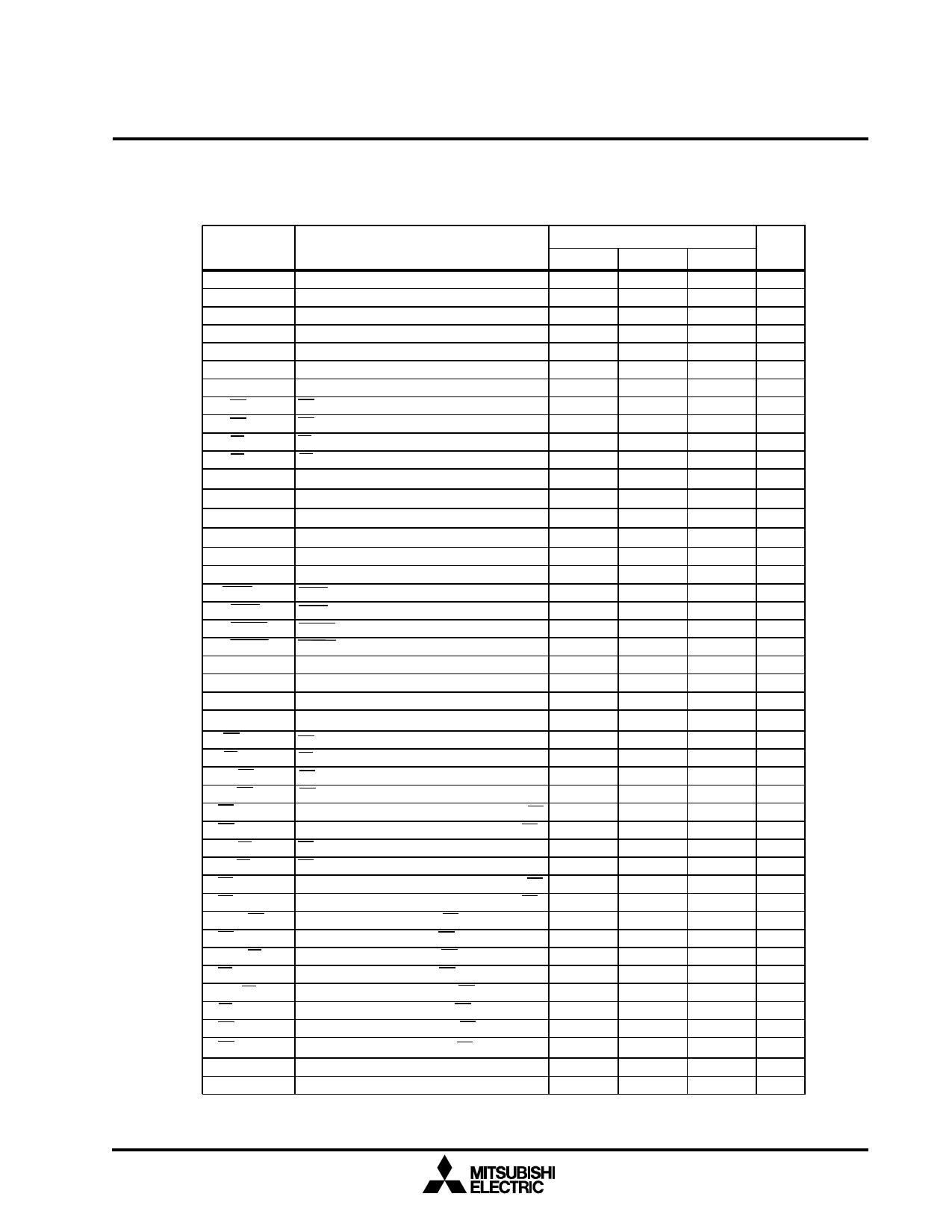
Table 2.5. Memory Expansion Mode and Microprocessor Mode Timing
(Vcc = 4.15 to 5.25V, Vss = 0V, Ta = -20 to 85°C unless otherwise noted)
Symbol
tc(Φ)
twh(Φ)
twl(Φ)
td(Φ-AH)
tv(Φ-AH)
td(Φ-AL)
tv(Φ-AL)
td(Φ-WR)
tv(Φ-WR)
td(Φ-RD)
tv(Φ-RD)
td(Φ-SYNC)
tv(Φ-SYNC)
td(Φ-DMA)
tv(Φ-DMA)
tsu(RDY-Φ)
th(Φ-RDY)
tsu(HOLD-Φ)
th(Φ-HOLD)
td(Φ-HLDAL)
tv(Φ-HLDAH)
tsu(DB-Φ)
th(Φ-DB)
td(Φ-DB)
tv(Φ-DB)
twl(WR)
twl(RD)
td(AH-WR)
td(AL-WR)
tv(WR-AH)
tv(WR-AL)
td(AH-RD)
td(AL-RD)
tv(RD-AH)
tv(RD-AL)
tsu(RDY-WR)
th(WR-RDY)
tsu(RDY-RD)
th(RD-RDY)
tsu(DB-RD)
th(RD-DB)
td(WR-DB)
tv(WR-DB)
tr(D+), tr(D-)
tf (D+), tf(D-)
Parameter
Min.
Φ clock cycle time
Φ clock “H” pulse width
Φ clock “L” pulse width
Address bus AB15-AB8 delay time with respect to Φ
Address bus AB15-AB8 valid time with respect to Φ
Address bus AB7-AB0 delay time with respect to Φ
Address bus AB7-AB0 valid time with respect to Φ
WR delay time
WR valid time
83.33
0.5*tc(Φ)-5
0.5*tc(Φ)-5
5
5
3
RD delay time
RD valid time
3
SYNCOUT delay time
SYNCOUT valid time
4
DMAOUT delay time
DMAOUT valid time
5
RDY setup time with respect to Φ
21
RDY hold time with respect to Φ
0
HOLD setup time
21
HOLD hold time
0
HLDAL delay time
HLDAH delay time
Data bus setup time with respect to Φ
7
Data bus hold time with respect to Φ
0
Data bus delay time with respect to Φ
Data bus valid time with respect to Φ (Note)
13
WR pulse width
RD pulse width
0.5*tc(Φ)-5
0.5*tc(Φ)-5
WR delay time after stable address AB15-AB8
WR delay time after stable address AB7-AB0
0.5*tc(Φ)-28
0.5*tc(Φ)-30
Address bus AB15-AB8 valid time with respect to WR
0
Address bus AB7-AB0 valid time with respect to WR
0
RD delay time after stable address AB15-AB8
0.5*tc(Φ)-28
RD delay time after stable address AB7-AB0
0.5*tc(Φ)-30
Address bus AB15-AB8 valid time with respect to RD
0
Address bus AB7-AB0 valid time with respect to RD
0
RDY setup time with respect to WR
27
RDY hold time with respect to WR
0
RDY setup time with respect to RD
27
RDY hold time with respect to RD
0
Data bus setup time with respect to RD
13
Data bus hold time with respect to RD
0
Data bus delay time with respect to WR
Data bus valid time with respect to WR Note
10
USB output rise time, CL=50 pF
4
USB output fall time, CL=50 pF
4
Note : Measurement conditions: Iohl = ±5ma, CL = 50pF
Limits
Typ.
Max.
31
33
6
6
6
25
25
25
22
20
20
20
Unit
ns
ns
ns
ns
ns
ns
ns
ns
ns
ns
ns
ns
ns
ns
ns
ns
ns
ns
ns
ns
ns
ns
ns
ns
ns
ns
ns
ns
ns
ns
ns
ns
ns
ns
ns
ns
ns
ns
ns
ns
ns
ns
ns
ns
ns
87
Share Link: 