L6382DTR View Datasheet(PDF) - STMicroelectronics
Part Name
Description
View to exact match
L6382DTR Datasheet PDF : 21 Pages
| |||
Pin settings
2
Pin settings
2.1
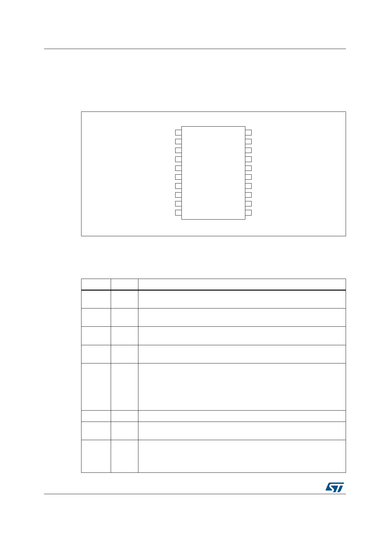
Pin connection
Figure 3. Pin connection (top view)
L6382D
2.2
4/21
3),
/6,
+6,
+(,
3)*
1&
735
*1'
/6*
9&&
95()
&6,
&62
+(*
1&
+968
1&
28 7
+6*
%22 7
$0
9
Pin description
Name
1
2
3
4
5
6
7
8
Table 1. Pin description
Pin no.
Description
PFI
Digital input signal to control the PFC gate driver. This pin must be connected
to a TTL compatible signal.
LSI
Digital input signal to control the half-bridge low-side driver. This pin must be
connected to a TTL compatible signal.
HSI
Digital input signal to control the half-bridge high-side driver. This pin must be
connected to a TTL compatible signal.
HEI
Digital input signal to control the HEG output. This pin must be connected to a
TTL compatible signal.
PFG
PFC driver output. This pin is intended to be connected to the PFC power
MOSFET gate. A resistor connected between this pin and the power MOS
gate can be used to reduce the peak current. An internal 10 k resistor toward
ground avoids spurious and undesired MOSFET turn-on. The totem pole
output stage is able to drive the power MOS with a peak current of 120 mA
source and 250 mA sink.
N.C. Not connected.
TPR
Input for two point regulator; by coupling the pin with a capacitor to a switching
circuit, it is possible to implement a charge circuit for the Vcc.
GND
Chip ground. Current return for both the low-side gate drive currents and the
bias current of the IC. All of the ground connections of the bias components
should be tied to a trace going to this pin and kept separate from any pulsed
current return.
DocID10972 Rev 8
Share Link: 