K4E641612D View Datasheet(PDF) - Samsung
Part Name
Description
View to exact match
K4E641612D Datasheet PDF : 36 Pages
| |||
Industrial Temperature
K4E661612D,K4E641612D
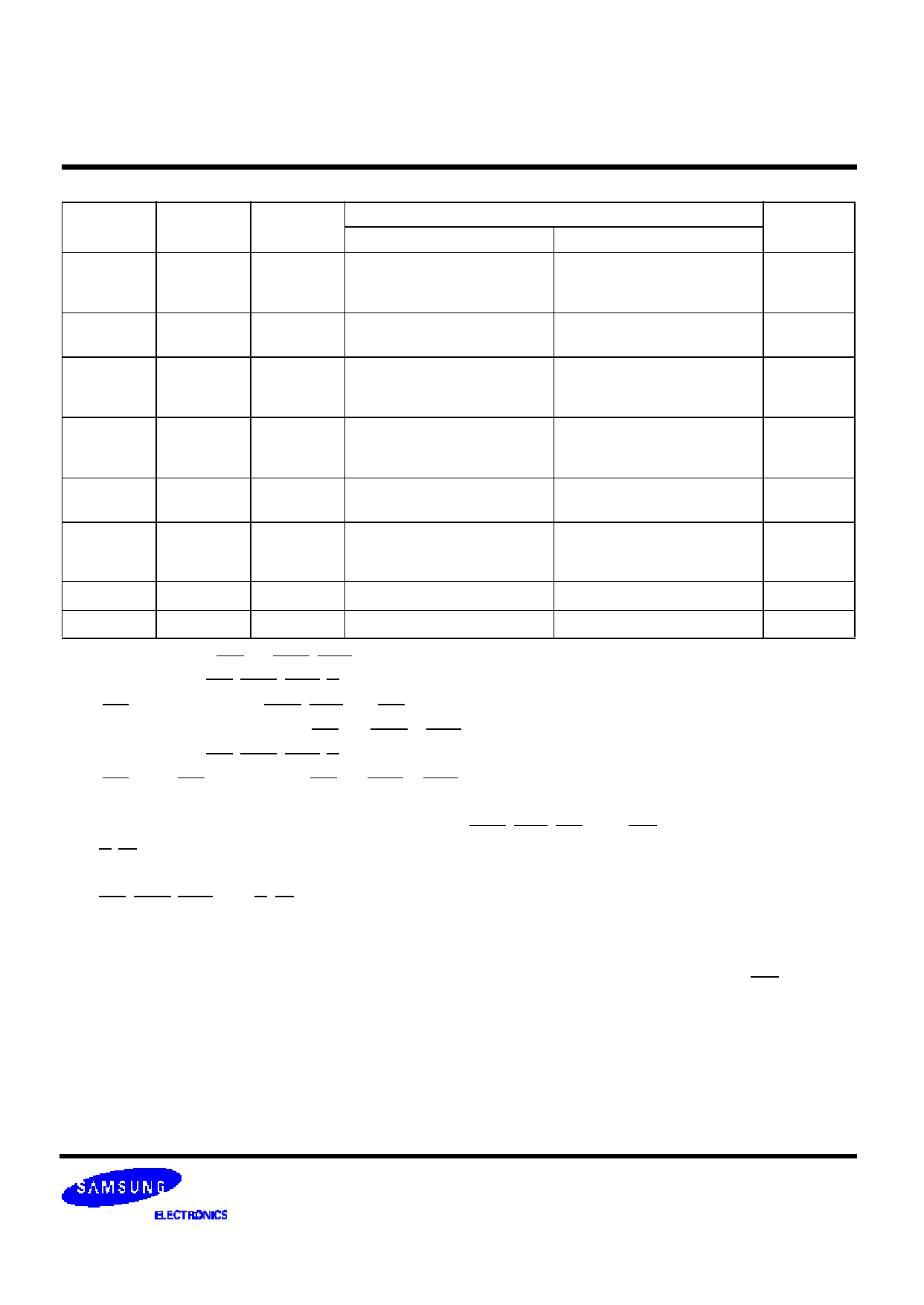
DC AND OPERATING CHARACTERISTICS (Continued)
Symbol
IC C 1
IC C 2
IC C 3
IC C 4
IC C 5
IC C 6
IC C 7
IC C S
Power
D o n ′t care
Normal
L
D o n ′t care
D o n ′t care
Normal
L
D o n ′t care
L
L
Speed
-45
-50
-60
D o n ′t care
-45
-50
-60
-45
-50
-60
D o n ′t c a r e
-45
-50
-60
D o n ′t c a r e
D o n ′t c a r e
K4E661612D
90
80
70
1
1
90
80
70
100
90
80
0.5
200
130
120
110
350
350
Max
CMOS DRAM
K4E641612D
130
120
110
1
1
130
120
110
100
90
80
0.5
200
130
120
110
350
350
Units
mA
mA
mA
mA
mA
mA
mA
mA
mA
mA
mA
mA
uA
mA
mA
mA
uA
uA
IC C 1* : O p e r a t i n g C u r r e n t ( R A S a n d U C A S , L C A S , A d d r e s s c y c l i n g @ t R C=min.)
IC C 2 : S t a n d b y C u r r e n t ( R A S = U C A S = L C A S = W = V IH )
IC C 3* : R A S - o n l y R e f r e s h C u r r e n t ( U C A S = L C A S = V IH , R A S , A d d r e s s c y c l i n g @ tR C = m i n . )
IC C 4* : E x t e n d e d D a t a O u t M o d e C u r r e n t ( R A S = V IL , U C A S o r L C A S , A d d r e s s c y c l i n g @ tH P C = m i n . )
IC C 5 : S t a n d b y C u r r e n t ( R A S= U C A S= L C A S =W = VCC - 0 . 2 V )
IC C 6* : C A S - B e f o r e - R A S R e f r e s h C u r r e n t (R A S a n d U C A S o r L C A S c y c l i n g @ t R C= m i n )
IC C 7 : B a t t e r y b a c k - u p c u r r e n t , A v e r a g e p o w e r s u p p l y c u r r e n t , B a t t e r y b a c k - u p m o d e
I n p u t h i g h v o l t a g e ( V IH ) = V C C - 0 . 2 V , I n p u t l o w v o l t a g e ( V IL ) = 0 . 2 V , U C A S , L C A S = C A S - b e f o r e - R A S c y c l i n g o r 0 . 2 V
W , O E = V IH , A d d r e s s = D o n ′t c a r e , D Q = O p e n , T R C = 3 1 . 2 5 u s
IC C S : S e l f R e f r e s h C u r r e n t
R A S= U C A S =L C A S = 0 . 2 V , W = O E= A 0 ~ A 1 2 ( A 1 1 ) = V C C- 0 . 2 V o r 0 . 2 V , D Q 0 ~ D Q 1 5 = V CC-0.2V, 0.2V or Open
* N o t e : IC C 1 , I C C 3 , IC C 4 a n d I C C 6 a r e d e p e n d e n t o n o u t p u t l o a d i n g a n d c y c l e r a t e s . S p e c i f i e d v a l u e s a r e o b t a i n e d w i t h t h e o u t p u t o p e n .
IC C i s s p e c i f i e d a s a n a v e r a g e c u r r e n t . I n I C C 1 , IC C 3 a n d I C C 6 , a d d r e s s c a n b e c h a n g e d m a x i m u m o n c e w h i l e R A S = V I L. I n I C C 4 ,
address can be changed maximum once within one EDO mode cycle time, tHPC.
Share Link: 