HT7730(2006) View Datasheet(PDF) - Holtek Semiconductor
Part Name
Description
View to exact match
HT7730 Datasheet PDF : 15 Pages
| |||
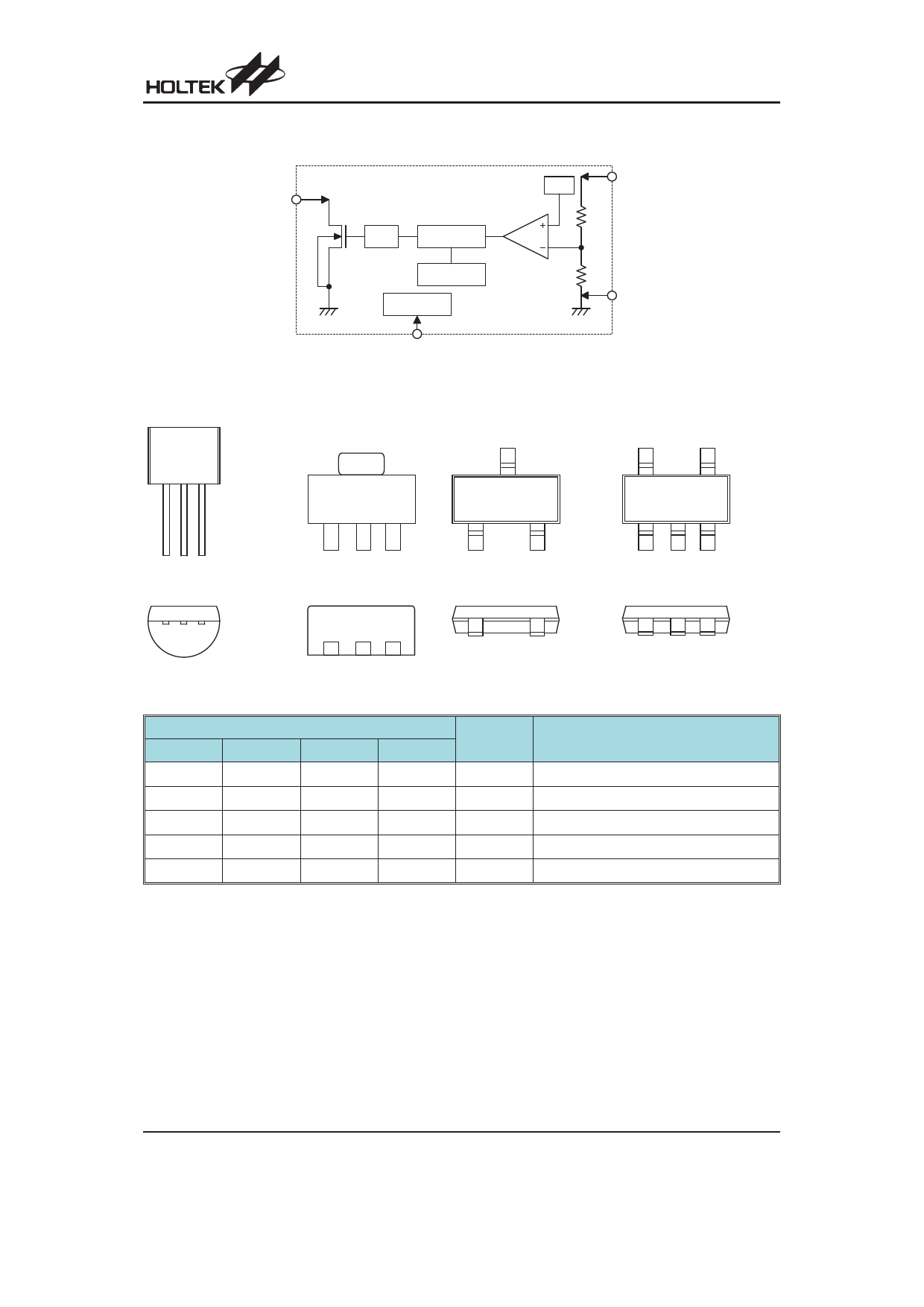
Block Diagram
LX
B u ffe r
P F M C o n tro l
O S C 115kH z
C h ip E n a b le
Pin Assignment
T O -9 2
CE
S O T -8 9
H T77X X
123
F r o n t V ie w
G N D V O U T LX
H T77X X
1
2
3
G N D V O U T LX
VO UT
V re f
HT77XX
GND
S O T -2 5
LX
GND
5
4
77X X
T o p V ie w
1
2
3
CE VO UT NC
B o tto m V ie w
G N D V O U T LX
CE VO UT NC
Pin Description
Pin No.
Pin Name
TO-92 SOT-25 SOT-89
Description
¾
1
¾
CE Chip enable pin, high active
2
2
2
VOUT DC/DC converter output monitoring pin
¾
3
¾
NC No connection
1
4
1
GND Ground pin
3
5
3
LX Switching pin
Absolute Maximum Ratings
Supply Voltage ..............................VSS-0.3V to VSS+7V
Power Consumption (*1) .................................. 500mW
Power Consumption (*2) .................................. 250mW
Storage Temperature ............................-50°C to 125°C
Operating Temperature...............................0°C to 70°C
Note: These are stress ratings only. Stresses exceeding the range specified under ²Absolute Maximum Ratings² may
cause substantial damage to the device. Functional operation of this device at other conditions beyond those
listed in the specification is not implied and prolonged exposure to extreme conditions may affect device reliabil-
ity.
*1: applied to SOT-89 and TO-92
*2: applied to SOT-25
Rev 1.10
2
March 7, 2006
Share Link: 