GS71116AJ View Datasheet(PDF) - Unspecified
Part Name
Description
View to exact match
GS71116AJ Datasheet PDF : 15 Pages
| |||
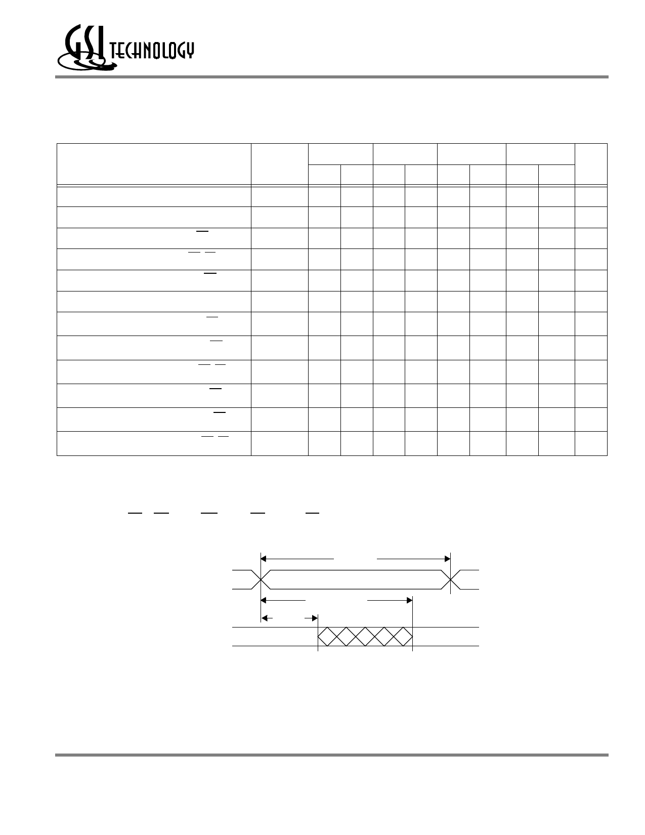
AC Characteristics
GS71116ATP/J/U
Read Cycle
Parameter
Read cycle time
Address access time
Chip enable access time (CE)
Byte enable access time (UB, LB)
Output enable to output valid (OE)
Output hold from address change
Chip enable to output in low Z (CE)
Output enable to output in low Z (OE)
Byte enable to output in low Z (UB, LB)
Chip disable to output in High Z (CE)
Output disable to output in High Z (OE)
Byte disable to output in High Z (UB, LB)
Symbol
tRC
tAA
tAC
tAB
tOE
tOH
tLZ*
tOLZ*
tBLZ*
tHZ*
tOHZ*
tBHZ*
-7
-8
-10
-12
Unit
Min Max Min Max Min Max Min Max
7 — 8 — 10 — 12 — ns
— 7 — 8 — 10 — 12 ns
— 7 — 8 — 10 — 12 ns
— 3 — 3.5 —
4
—
5
ns
— 3 — 3.5 —
4
—
5
ns
3—3—3
—
3
— ns
3—3—3
—
3
— ns
0—0—0
—
0
— ns
0—0—0
—
0
— ns
— 3.5 — 4 —
5
—
6
ns
— 3 — 3.5 —
4
—
5
ns
— 3 — 3.5 —
4
—
5
—
* These parameters are sampled and are not 100% tested.
Read Cycle 1: CE = OE = VIL, WE = VIH, UB and, or LB = VIL
Address
Data Out
tOH
Previous Data
tRC
tAA
Data valid
Rev: 1.04a 10/2002
7/15
© 2001, Giga Semiconductor, Inc.
Specifications cited are subject to change without notice. For latest documentation see http://www.gsitechnology.com.
Share Link: 