HD74CDCV857 View Datasheet(PDF) - Hitachi -> Renesas Electronics
Part Name
Description
View to exact match
HD74CDCV857 Datasheet PDF : 13 Pages
| |||
HD74CDCV857
Recommended Operating Conditions
Item
Symbol Min
Typ
Max
Unit Conditions
Supply voltage
Output supply voltage
DC input signal voltage *1
High level input voltage
Low level input voltage
Differential input signal voltage
Differential cross point voltage *2
Output current
Input slew rate
AVCC
VDDQ
VIHG
VILG
VID
VIX
V *3
OX
I OH
I OL
SR
2.3
2.5
2.3
2.5
–0.3
—
1.7
—
–0.3
—
0.36
—
0.5×VDDQ —
–0.20
—
—
—
—
1
—
2.7
V
2.7
V
VDDQ+0.3 V
VDDQ+0.3 V
0.7
V
All pins
PWRDWN input pin
PWRDWN input pin
VDDQ+0.6 V
0.5×VDDQ V
+0.20
–12
mA
12
4
V/ns 20% – 80%
Operating temperature
Ta
0
—
70
°C
Notes: Inputs pins must be prevent from floating.
Feedback inputs (FBIN, FBIN) may float when the device is in low power mode.
1. DC input signal voltage specifies the allowable dc execution of differential input.
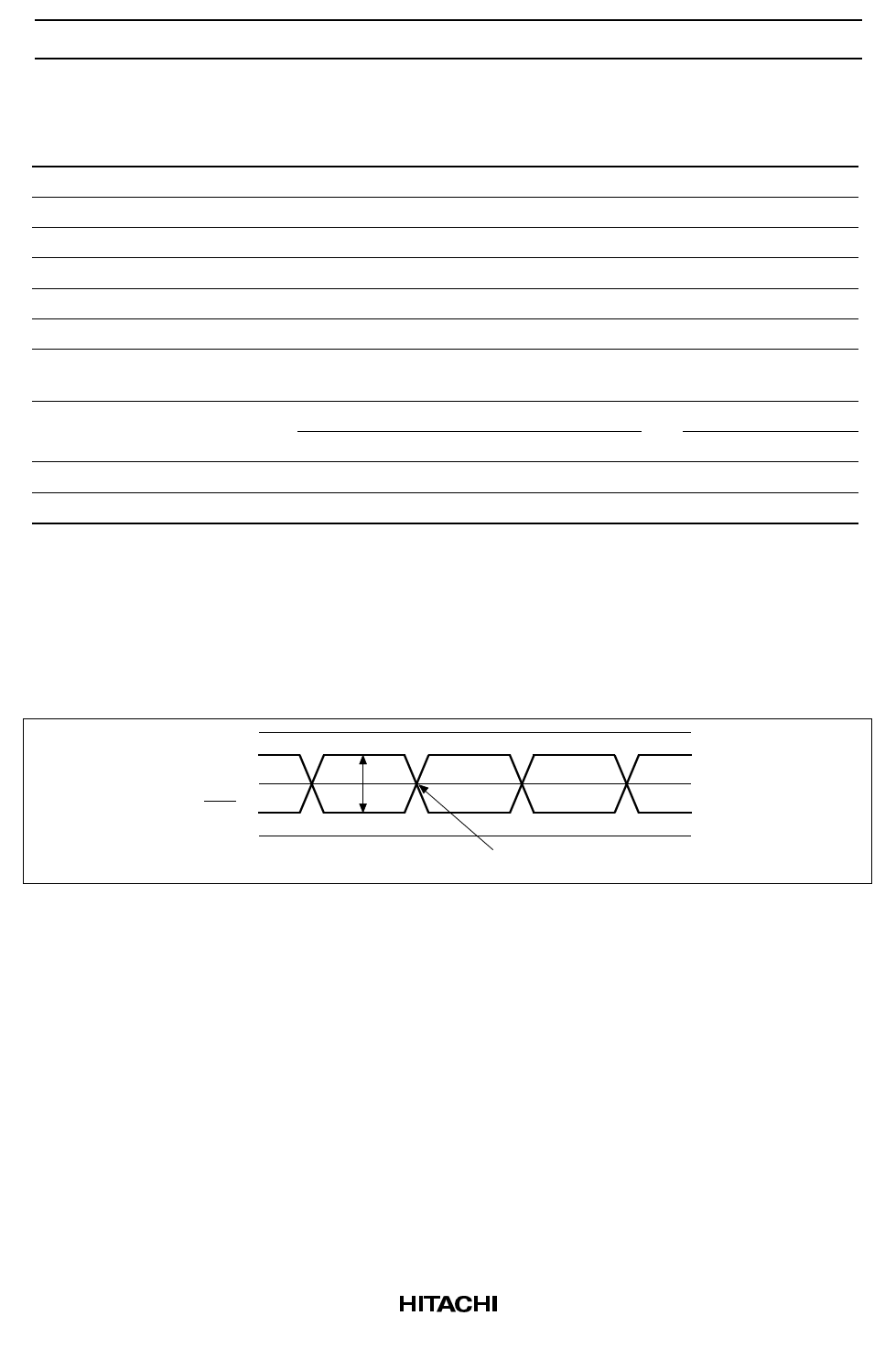
2. Differential cross point voltage is expected to track variations of VDDQ and is the voltage at which
the differential signals must be crossing. (See figure1)
3. Guaranteed by design, not 100% tested in production.
CLK
VID
CLK
Crossing point
Figure 1 Differential input levels
6
Share Link: 