AD8153 View Datasheet(PDF) - Analog Devices
Part Name
Description
View to exact match
AD8153 Datasheet PDF : 24 Pages
| |||

Data Sheet
ABSOLUTE MAXIMUM RATINGS
Table 3.
Parameter
VCC to VEE
VTTI
VTTO
Internal Power Dissipation
Differential Input Voltage
Logic Input Voltage
Storage Temperature Range
Lead Temperature
Junction Temperature
Rating
3.7 V
VCC + 0.6 V
VCC + 0.6 V
4.1 W
2.0 V
VEE − 0.3V < VIN < VCC + 0.6 V
−65°C to +125°C
300°C
150°C
AD8153
Stresses at or above those listed under Absolute Maximum
Ratings may cause permanent damage to the product. This is a
stress rating only; functional operation of the product at these
or any other conditions above those indicated in the operational
section of this specification is not implied. Operation beyond
the maximum operating conditions for extended periods may
affect product reliability.
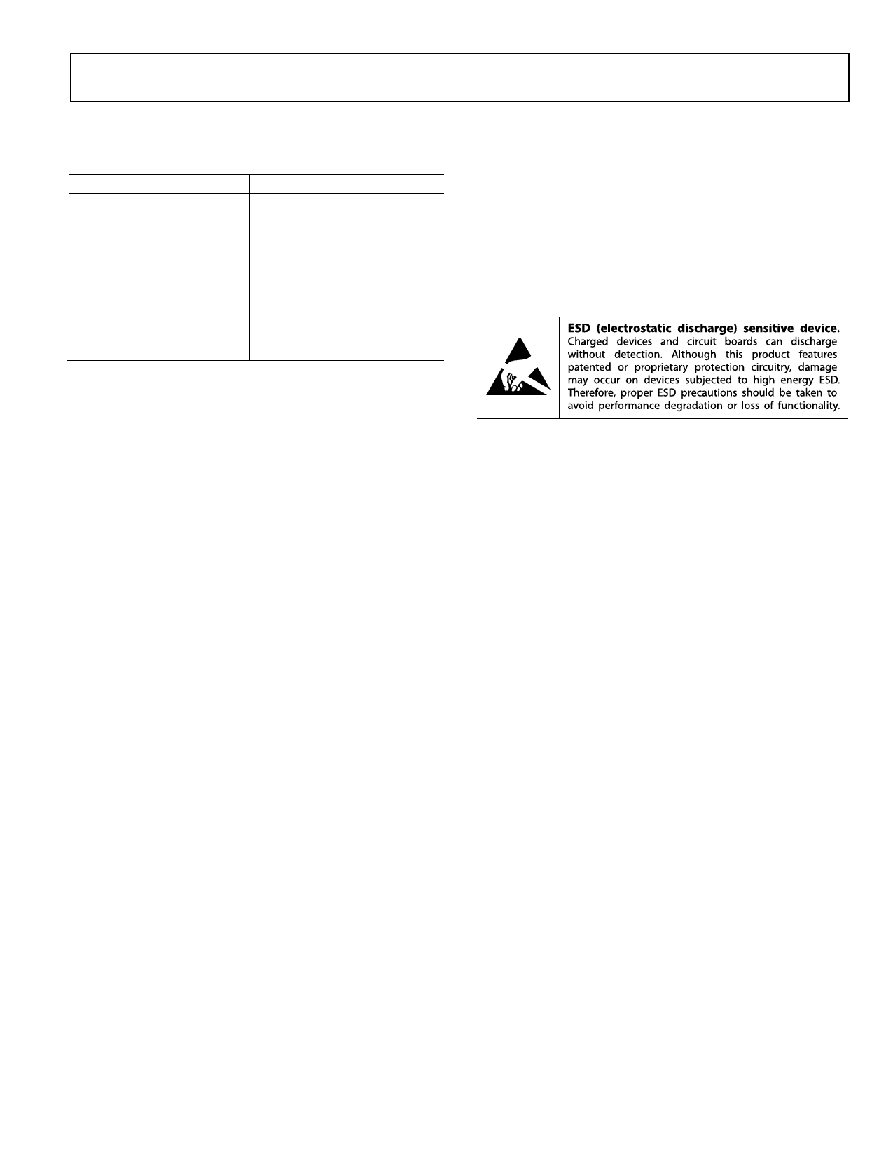
ESD CAUTION
Rev. A | Page 5 of 24