NJU6682CH View Datasheet(PDF) - Japan Radio Corporation
Part Name
Description
View to exact match
NJU6682CH Datasheet PDF : 58 Pages
| |||
NJU6682
No Symbol
50
C0
to
to
209
C159
341
S0
to
to
210
S131
I/O
Function
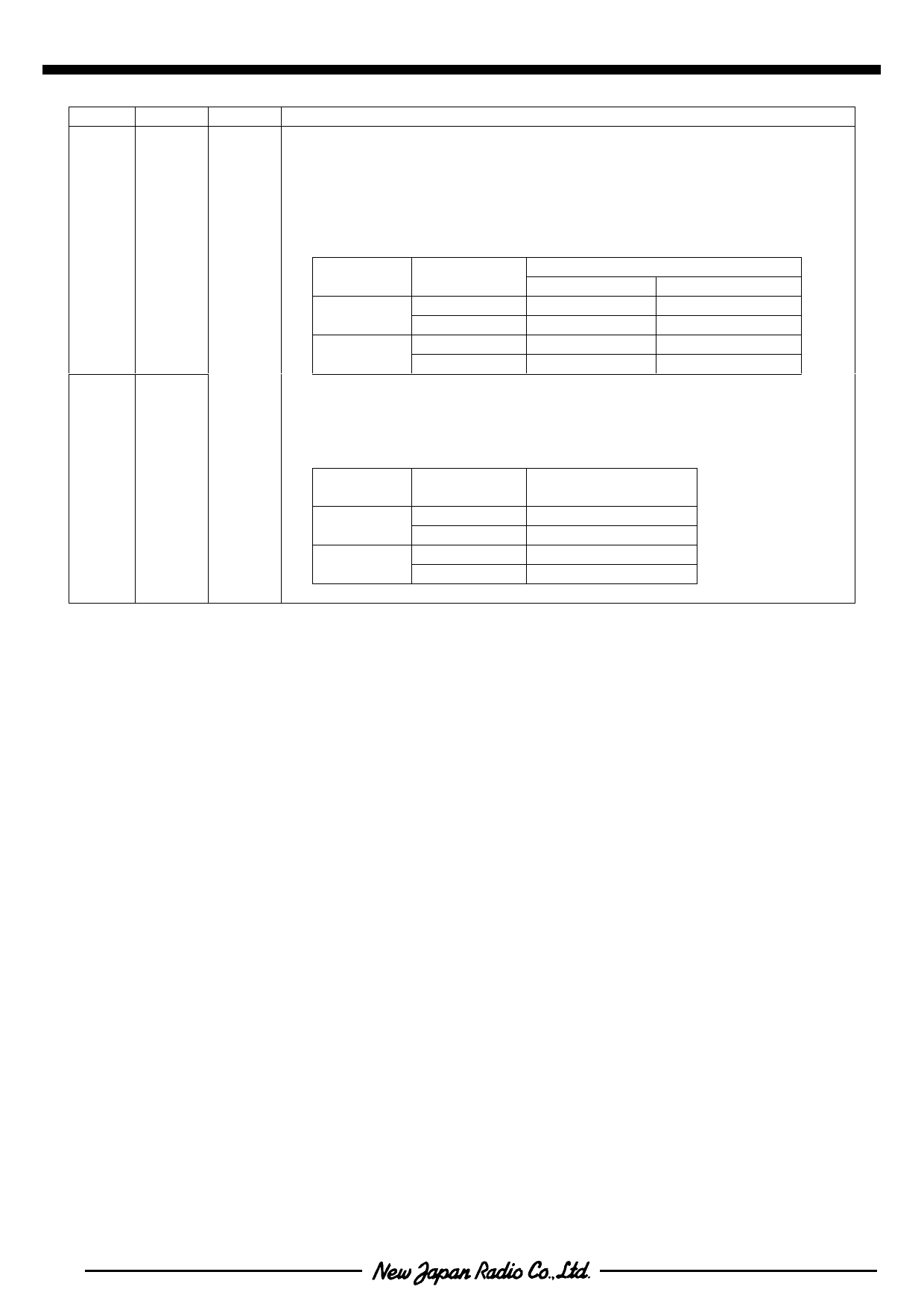
LCD driving signal output terminal.
•Common output terminal :C0 to C159
•Segment output terminal :S0 to S131
•Segment output terminal
The following output voltage are selected by the combination of
FR and data in the RAM.
O
RAM Data Alternating
Sn OutPut Voltage
Signal
Disp. Positive
Disp. Negative
H
VDD
V2
H
L
V5
V3
L
H
V2
L
V3
VDD
V5
•Common output terminal
The following output voltage are selected by the combination of FR
and status of common.
Scan Data
H
L
Alternating
Signal
H
L
H
L
COn Output Voltage
V5
VDD
V1
V4
Share Link: 