KKA8133A View Datasheet(PDF) - Kodenshi Auk Co., LTD
Part Name
Description
View to exact match
KKA8133A Datasheet PDF : 4 Pages
| |||
KKA8133A
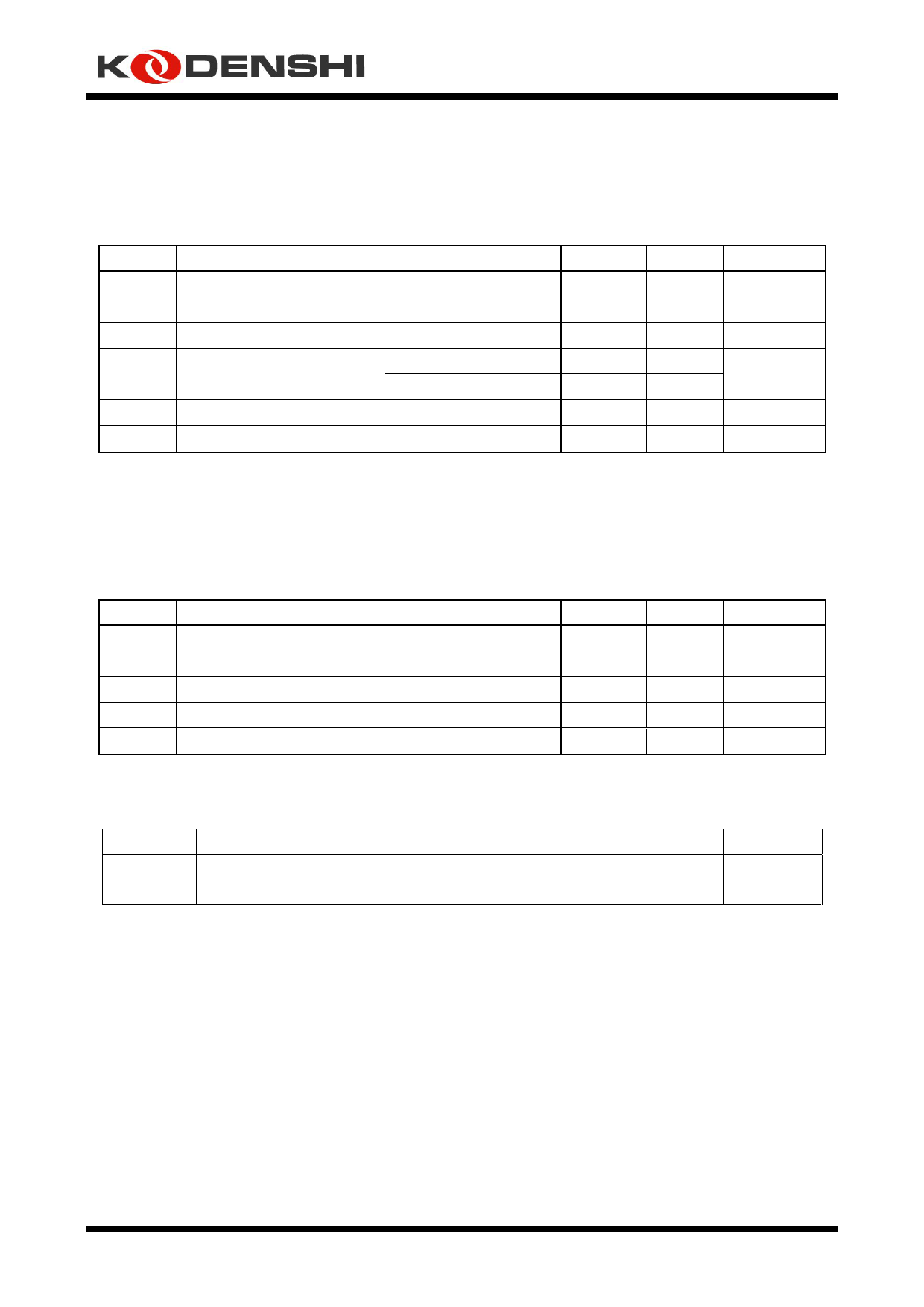
MAXIMUM RATINGS*
Symbol
Parameter
Min
Max
Unit
VIN1 DC Input Voltage Pin 1
20
V
VIN2 DC Input Voltage Pin 2
20
V
VDIS Disable Input Voltage Pin 3
20
V
IO1,2 SC
Short Circuit Output Current VIN1 = 7 V, VIN2 = 10 V
1.6
A
VIN1 = VIN2 = 16 V
1.0
Tstg Storage Temperature
-65
150
°C
TJ
Junction Temperature
0
150
°C
*Maximum Ratings are those values beyond which damage to the device may occur.
Functional operation should be restricted to the Recommended Operating Conditions.
RECOMMENDED OPERATING CONDITIONS
Symbol
VIN1
VIN2
VDIS
IO1,2
TJ
Parameter
DC Input Voltage Pin 1
DC Input Voltage Pin 2
Disable Input Voltage Pin 3
Output Currents
Junction Temperature
THERMAL DATA
Symbol
Rth (j-c)
Rth (j-a)
Parameter
Maximum Thermal Resistance Junction-case
Maximum Thermal Resistance Junction-ambient
Min
Max
Unit
7.0
14
V
10
14
V
0
7.0
V
1.0
A
0
130
°C
Vlalue
6
60
Unit
oC/W
oC/W
2
Share Link: 